It's time for another GAMBICA guest blog! This new project will allow members to create content about an industry issue that’s important to them. Whether it’s the skills gap, sustainability in our sectors or the importance of standards – we can’t wait to share more thoughts from our members through this platform.
This edition we hear from member Paragraf, the first company in the world to mass produce graphene-based electronic devices using standard semiconductor processes.
The emergence of GFETs within and beyond the laboratory environment
Graphene field-effect transistors (GFETs) are an emerging sensing technology with applications in ion detection, environmental monitoring, and healthcare diagnostics. Their combination of compact size, high sensitivity and rapid response times makes them an appealing addition to lab equipment designed for chemical and biological analysis. Additionally, these factors lend themselves well to point of care diagnostics and lab-on-chip applications, such as biofluid testing, expanding the laboratory’s reach beyond its traditional confines.
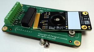
(Image - Paragraf GFET molecular sensor with a PiG Breakout Board for pairing with data acquisition system.)
How Graphene is Overcoming Manufacturing Challenges
One of the challenges of incorporating graphene into sensing devices has been maintaining consistent material quality. Early manufacturing techniques often relied on transferring graphene layers grown by chemical vapor deposition (CVD) onto a substrate, which introduced defects and contamination, limiting the sensitivity and reliability of the sensors.
An alternative approach developed at Paragraf is to avoid the transfer process completely using modified metal-organic chemical vapor deposition (MOCVD) equipment to enable direct growth of graphene on semiconductor-compatible substrates such as silicon and sapphire. This method reduces contamination and ensures greater reproducibility in sensor fabrication, making it a more suitable process for large-scale production of GFET-based sensing components.
How GFETs Enable High-Sensitivity Detection
GFETs function by detecting changes in electrical conductivity across a sheet of graphene, allowing them to measure subtle variations in current. This enables the detection of specific molecules in gases or liquids.
In electrolyte-gated GFETs, a sample droplet is placed on the sensing surface, enabling an electrical bias to be applied between the gate electrode and the graphene channel. This bias shifts the doping level of graphene, affecting its electronic properties. The resulting changes in conductivity can be used to determine key characteristics such as ion concentration, pH levels and biomarker presence. Graphene’s exceptional conductivity and electron mobility provide a reliable and sensitive solution that tests have proven competitive with other technologies.
Surface modifications can further enhance GFET specificity. By functionalizing the graphene surface with targeted receptors or chemical groups, GFETs can be adapted to detect a wide range of analytes, from single ions to complex biological molecules.
Potential Integration into Existing Lab Environment
GFET technology can be incorporated into a variety of current lab instrumentation, particularly those requiring sensitive detection of chemical and biological targets. Some potential applications include:
- Healthcare diagnostics: GFETs can be functionalized with bioreceptors to detect disease markers in biofluids.
- Environmental monitoring: Their sensitivity to ion concentration changes makes them suitable for water quality analysis and pollutant detection.
- Chemical analysis: GFETs can detect small variations in molecular composition, enabling precise material characterization.
In addition, multiplexing—the ability to integrate multiple GFET sensors on a single chip—offers the possibility of simultaneously measuring several analytes within a single test. This could enhance the efficiency of high-throughput screening and complex sample analysis in laboratory settings.
The Lab Outside the Lab
The portability and versatility of GFETs enable point-of-care diagnostics and field sampling, extending their application beyond traditional laboratory settings. This capability reduces reliance on bulky lab-based apparatuses and processes. However, it also necessitates the development of compatible interfacing tools tailored to field conditions.
Specifically, the GFET requires partner instruments that can translate its signals and deliver actionable readings. These instruments would need to boast a similar portability to the GFET itself, independent power supply and a robustness that allow them to operate in potentially unfriendly circumstances. They would also have to provide user-friendly interfaces to make full use of the immediacy of the results GFET sampling provides and, ideally, they would also feature internet connectivity to access relevant records, subject-matter experts and regulatory bodies in real time.
Further Considerations for Equipment Integration
For manufacturers looking to integrate GFETs into lab equipment, several factors should be considered:
- Material compatibility: Ensuring that GFETs can be incorporated into existing device architectures without introducing contamination or stability issues.
- Scalability: Current production methods allow for multiple GFETs to be fabricated on a single wafer, with potential for further scaling.
- Reproducibility and calibration: Like other sensors, GFETs must deliver consistent performance across batches, requiring stringent manufacturing and calibration protocols.
Addressing these challenges requires collaboration between Paragraf, equipment manufacturers and healthcare providers to create integrated solutions that leverage the sensitivity of GFETs while meeting the practical demands of point-of-care testing.
As research into GFETs continues, their capabilities and integration strategies are expected to evolve. By understanding their properties and manufacturing considerations, lab equipment developers can assess how these sensors might enhance their devices for various analytical applications.